Department of Electrical and Computer Engineering
ECED 4260 IC Design and Fabrication
Project A. Arithmetic Logic Unit - GCD Calculator
OBJECTIVES
- To Design and Implement an Arithmetic Logic Circuit
- Integrate a behavioral control path and a structural data path in a single design
- Implement a digital system using HDL and DE1-SoC boards and observe the operation
Design Problem
Consider the 4-bit Arithmetic Logic Unit (ALU) below:
This design lab will solve the GCD (greatest common divisor) problem. That is
to take two 4-bit unsigned binary numbers, a and b, and compute their greatest
common divisor, the largest number that will divide evenly into both numbers.
The digital system is implemented on the FPGA boards.
To solve the GCD problem, the following GCD algorithm was used:
function gcd(u,v)
load u and v;
while u /= v do
if u > v then
u := u - v;
else
v := v - u;
end if;
end while;
output u or v;
end gcd;
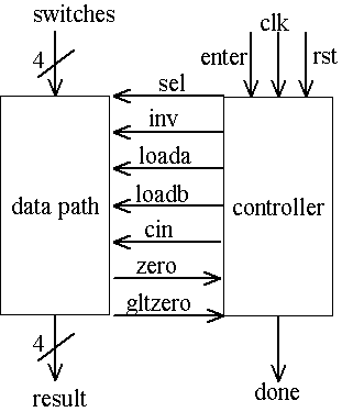
The final digital system should be like this:
1) When the system is first powered up, the user shall press the RESET push button to force the system into initial state. Then the user uses a set of four toggle switches to input the two numbers a and b. (Note: a and b can not be zero input. )
2) The system accepts a when the enter push button (active low) is pressed, same as number b.
3) The system calculates the GCD of the two numbers after the two numbers are accepted. Four LEDs labeled L3-L0 display the results.
4) An LED labeled DONE indicates that the first GCD calculation has been computed. Then subsequent GCDs may be computed using the same procedure.
The Lab Assignment
The design will be composed of a distinct control path and data path, which
will be put together and programmed into a FPGA.
Part I: Data Path
There are also some constraints for the data path design. First is that data path should be designed structurally. Second is that behavioral or other explicit comparator operations cannot be used within design, and only one 4-bit adder and four two-input XOR gates are allowed within code for the data path.
Base on the algorithm, we can design the data path: Two binary numbers are input to the system through four switches. There are three primary operations taking place after the loading of the initial values:
- Comparison of the values u and v.
- Subtraction of one number from another.
- Assignment of the difference to either the u or v register.
The following data path diagram can be derived from the above algorithm:
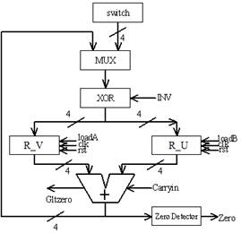
The algorithm can be distilled into the following processes:
- If the sum of the register v and -u is greater than zero, that sum is placed un-inverted into the v register.
- If the sum of the register v and -u is less than zero, that sum is placed into the u register.
- If the sum is zero, the algorithm is done and the result can be found in either the -u or v registers (since the difference is zero, one result is inverted and the other is not).
Therefore the three operations of comparison, inversion, and assignment are accomplished as follows:
- Comparison - The comparison result comes from the carry out of the adder. (The zero detection should be fairly obvious).
- Inversion - The 2's complement of a number is found by XOR-ing the number bit-wise with a 1, and then adding a 1 afterwards using the carry in of the adder.
- Assignment - when the sum is presented, it is loaded into one of the u or v registers as the algorithm requires.
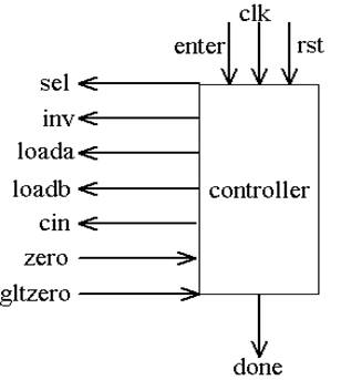
Part II: Control Path
Part III: Final Design
Part IV: Hardware Implementation
As a portion of this lab involves actual implementation of a digital system in hardware, it is important that several important points be made about how to handle this hardware. Large transient voltages such as those present with static electricity can permanently damage the FPGAs. In short, you must take special precautions in handling the FPGA boards and preventing the buildup of static electricity on your body.
Final Report
- The preparing elements from Part I and Part II.
- Your HDL code from Part I and Part II
- Your annotated waveforms from Part I and Part II.
- Your experimental results from Part III (Simulation and DE1-SoC Board Implementation)
- Answer the lab questions in the body of your report if there is any.